This article has been reviewed according to Science X's editorial process and policies. Editors have highlighted the following attributes while ensuring the content's credibility:
fact-checked
proofread
Researchers improve the performance of semiconductors using novel 2D metal

Two-dimensional transition-metal dichalcogenides (2D TMDs), especially MoS2, are at the forefront of new-generation 2D materials, and industrial-level efforts are being made to produce them at a large scale with reasonable performance for electronic device applications. Usually, for display applications, charge carrier mobility of 2 cm2/V.s is sufficient.
Though mechanically exfoliated MoS2 is well-known to have much higher mobility than this, its large-area production is challenging. Further, it is unclear how the performance of 2D TMD devices will be if they are contacted by new generation 2D metals instead of standard 3D metals such as Au, Ti, Ni, etc.
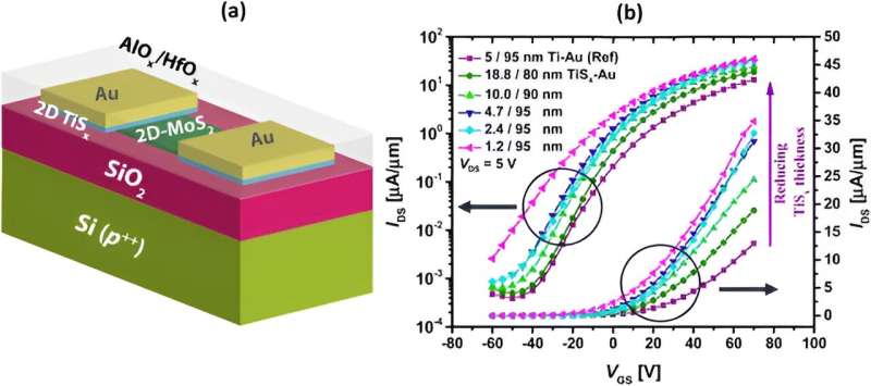
Hence, researchers at Eindhoven University of Technology (Tue), The Netherlands and SRM Institute of Science and Technology (SRMIST), India, have reported recently in Nanoscale Advances on the large-area growth of 2D metal TiSx on top of 2D semiconductor MoS2 by plasma-enhanced atomic layer growth (PEALD) technique.
It's very challenging to optimize the growth conditions to obtain an atomically clean interface between such materials. Researchers found that the transistor performance of MoS2 is almost two times better when contacted with the 2D metal TiSx compared to Ti and Au 3D metals. The trend was observed in most of the figures-of-merit of the transistor. This procedure can be utilized for many such materials in the future.
The charge transport study at various temperatures revealed variations in the meta-semiconductor junction barrier height and its impact on contact resistance. To understand this new system, researchers performed TCAD device simulation to visualize the distribution of charge carriers in atomic layers. It is noticed that in the presence of TiSx, the intrinsic charge carrier density of MoS2 increases, which leads to improved performance.
These results will allow the metallic contacts in 2D and 3D device integration to be thinned down, increasing device density. This exemplary research will play an important role in future quantum devices and in identifying new charge transport equations across the interface of 2D metal-semiconductors.
More information: Reyhaneh Mahlouji et al, ALD-grown two-dimensional TiSx metal contacts for MoS2 field-effect transistors, Nanoscale Advances (2023). DOI: 10.1039/D3NA00387F
Provided by SRM Institute of Science and Technology


